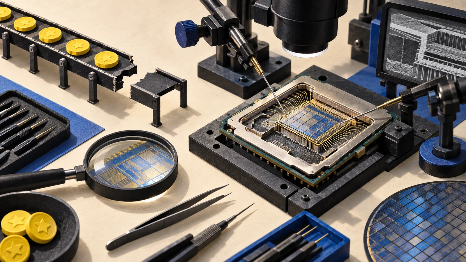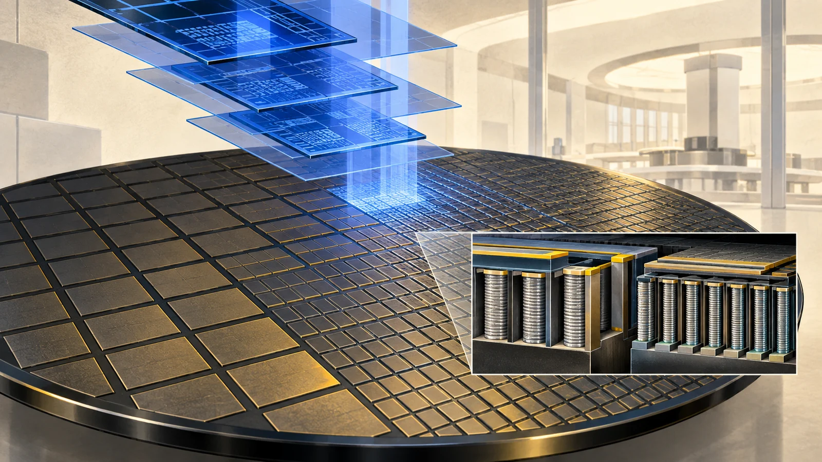
China’s largest DRAM maker says its fifth-generation manufacturing platform has entered mass production, a concrete test of whether the country’s memory industry can turn technical catch-up into competitive supply. The headline number is striking: CXMT says the new process can fit at least 50% more gross memory dies on a wafer than its previous platform. The important word is gross.
CXMT announced the G5 platform on September 20 at the World Manufacturing Convention in Hefei. The company reports an active-area half-pitch of 11.95 nanometers, a 45-to-1 capacitor aspect ratio, and a smaller core-cell-array height. It also unveiled two 24-gigabit LPDDR5X chips for phones and portable electronics, which it says are already in mass production and hold 50% more data than its previous equivalent products.
Four patterns make one smaller pattern
The technical hinge is self-aligned quadruple patterning. Instead of relying on one exposure to print every tiny feature, manufacturers use a sequence of deposition and etching steps to multiply a larger pattern into narrower, more closely spaced lines. It is a way to keep shrinking structures when the most advanced lithography tools are unavailable or uneconomic.
That ingenuity has a bill. More patterning steps mean more opportunities for alignment errors, defects, longer production cycles, and added process cost. Smaller features are useful only when enough finished dies pass testing at the required speed and power. A wafer crowded with candidates is not the same thing as a tray full of sellable chips. Semiconductor manufacturing remains rude enough to grade the homework.
Reuters noted that CXMT’s 50% comparison counts potential dies before defective units are removed and is normalized to an 8-gigabit design. The company has not disclosed production yield, tested performance, customer qualification results, output volume, or manufacturing cost. Those omissions do not erase the density advance, but they limit what the announcement proves.
The node label is not the whole chip
The reported 11.95-nanometer figure describes a particular spacing inside the memory array. It should not be read as a drop-in equivalent to the marketing names attached to every rival process. BusinessKorea similarly cautioned that the dimension is not directly comparable with the process-node labels used by Samsung and SK hynix. Its reporting placed the announcement in a competitive context while noting industry estimates that CXMT still trails those companies when yield, process stability, and cost are considered together.
The strongest counterargument is therefore straightforward: CXMT has published company measurements and a production declaration, not an independently audited manufacturing scorecard. Established suppliers already operate enormous qualified supply chains, and leading memory competition increasingly includes high-bandwidth memory for AI accelerators, not only mobile DRAM. A denser LPDDR5X platform does not establish parity across the market.
Still, this is more than a laboratory slide. A process that reaches volume production, supports shipping products, and raises die density can improve the economics of ordinary memory even without winning the performance crown. If CXMT can sustain acceptable yields, buyers gain another source and incumbents face pressure in the mobile and conventional DRAM segments where scale and price matter.
TINA’s view: believe the milestone, audit the economics
TINA’s view: CXMT’s announcement is credible evidence of meaningful process progress, but not yet proof that China has closed the DRAM manufacturing gap. The defensible conclusion is narrower and still important: quadruple patterning has produced a denser platform that the company says is running in volume, despite trade restrictions intended to slow access to advanced chipmaking capability.
This judgment would strengthen with independent teardowns, sustained customer shipments, disclosed yields, and evidence that the 24-gigabit parts meet their promised power and speed at competitive cost. It would weaken if qualification stalls, usable yields remain low, or the extra patterning steps consume the density advantage in time and expense.
The next signal is not another nanometer comparison. Watch which phone makers ship these chips, at what volume, and whether market pricing or rival product plans move in response. The wafer diagram says CXMT can draw more boxes. The market will decide how many of them work.